首页 / 品质体系Home / Quality

品质是设计出来的,不是检验出来的Quality is Designed In, Not Inspected In

从体系认证到八道检验关口,每一片板卡都在同一套标准下生产与追溯。From certified systems to eight inspection gates, every board is produced and traced under one standard.

▣ 01 · 认证体系▣ 01 · CERTIFICATIONS

权威认证,行业认可Certified, Industry-Trusted

通过汽车、医疗与通用电子等多行业体系认证,覆盖不同客户的合规要求。Certified across automotive, medical and general electronics to meet every compliance need.

QISO9001:2015

质量管理体系基础认证,覆盖设计、生产到交付全流程。Foundation QMS covering design, production and delivery.

AIATF16949

汽车行业质量管理体系,支持 PPAP / APQP 要求。Automotive QMS supporting PPAP / APQP requirements.

MISO13485

医疗器械质量管理体系,全流程文档与记录受控。Medical device QMS with controlled documentation.

IPIPC-A-610

电子组件验收标准,作业与检验严格按 IPC 执行。Electronic assembly acceptance per IPC workmanship standards.

RRoHS / REACH

无铅制程与有害物质管控,提供合规声明文件。Lead-free process and hazardous substance control with compliance docs.

UUL / CE

支持北美与欧盟市场准入的合规与测试协助。Compliance and testing support for North America & EU.

▣ 02 · 八道检验关口▣ 02 · EIGHT INSPECTION GATES

每道工序,先检后用Every Step, Checked Before Use

问题在源头被拦截,而不是在出货时被发现。Defects are caught at the source, not at shipment.

GATE 01
IQC 来料检验Incoming QC
元件与 PCB 来料全检,杜绝不良品流入产线Full inspection of parts & boards
GATE 02
SMT 首件确认First-Article
首件全参数比对,确认无误后批量投产Full parameter sign-off before volume
GATE 03
印刷 3D SPI3D SPI
锡膏高度与偏移 3D 检测,印刷不良拦截Paste height & offset screening
GATE 04
炉前 AOIPre-Reflow AOI
贴装偏移与缺件在回流前即时发现Placement defects before reflow
GATE 05
炉后 AOIPost-Reflow AOI
焊点质量全检,虚焊立焊一目了然Full solder-joint inspection
GATE 06
X-Ray 检测X-Ray
BGA 空洞率与桥接检测,符合 IPC-7095BGA voiding per IPC-7095
GATE 07
ICT / FCTICT / FCT
电路与功能双重测试,数据单板留存Circuit & function test, data archived
GATE 08
OQC 出货检验Outgoing QC
外观 AQL 抽检 + 包装核查,合格方可出货AQL sampling & packaging check
▣ 03 · 检验现场▣ 03 · INSPECTION FLOOR

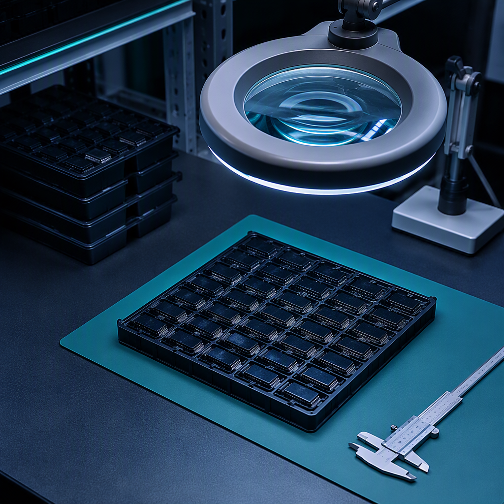
每一道关,看得见Every Gate, Visible

从来料到出货,检验工位全天运转,记录全程留档。From incoming to outgoing, inspection stations run around the clock with full records.

▣ 04 · 品质数据▣ 04 · QUALITY METRICS

用数据定义品质Quality, Defined in Numbers

0%出货直通率First-Pass Yield
0+关键工序 CPKKey Process CPK
0%批次可追溯Batch Traceability
0<%客户投诉率Customer Complaint Rate
全流程数据留档 · 支持随货提供 COC / 检测报告Full data archive · COC & test reports available with shipment
▣ 05 · 常见问题▣ 05 · FAQ

你可能想问的问题Questions You May Ask

PCB 打样通常 3–5 天,SMT 小批量一般 5–7 天,具体视物料交期与工艺复杂度而定,可加急。PCB prototypes typically take 3–5 days and SMT low-volume 5–7 days, depending on materials and complexity. Expediting is available.
可以。下单前发送 Gerber 文件,工程团队免费进行可制造性分析并出具报告,提前规避问题。Yes. Send your Gerber before ordering and our engineers run a free manufacturability analysis with a report.
两种模式都支持:来料加工(客户供料)、全包模式(我方采购),也可以混合搭配。Both are supported: consignment (your parts) or turnkey (we source). A mix is also fine.
可以。每片板卡的测试数据均留档保存,批次与单板均可追溯,可随货提供检验报告。Yes. Test data for every board is archived and unit/batch traceable, with inspection reports available.
支持。通过 DHL / FedEx 等渠道发往全球 30+ 国家,可协助出口清关与单证办理。Yes. We ship via DHL/FedEx to 30+ countries and can assist with customs and export documentation.

还有更多问题?More Questions?

直接与我们对话,工程团队将在 24 小时内回复。Talk to us directly — our engineers reply within 24 hours.